 Wus Printed Circuit Rises After Unveiling USD300 Million High-End PCB Investment
(Yicai) Jan. 13 -- Shares of Wus Printed Circuit rose against the market today after the Chinese maker of equipment for data centers and communications announced plans to invest a total of USD300 million to develop and mass-produce high-density optoelectronic integrated circuit boards (OEIC) used in artificial intelligence computing and autonomous driving.
Wus Printed Circuit [SHE: 002463] closed 0.5 percent elevated at CNY69.44 (USD10) today after rising as much as 4.2 percent intraday. Meanwhile, China’s major stock indexes retreated after several consecutive days of gains, with the Shenzhen Component Index ending the day down 1.4 percent.
The project will be built in Changzhou, in eastern China’s Jiangsu province, the Kunshan-based firm announced yesterday. It will be developed in two phases, with the first focusing on research and development and pilot production of high-density OEIC, before expanding capacity to large-scale production once market demand is verified.
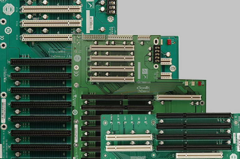
High-density OEICs integrate high-speed PCBs with optoelectronics to transmit electrical and optical signals for AI, data centers, communications, medical, and aerospace uses.
Wus Printed Circuit’s investment underscores the printed circuit board company’s push into advanced interconnection technologies as demand grows from emerging sectors such as AI, data centers, and high-speed optical communications.
After the project is fully completed, annual output is expected to reach 1.3 million high-density OEIC, generating annual sales of CNY2 billion (USD280 million) and pre-tax profit of more than CNY300 million (USD42 million), according to the announcement.
Construction Plan
The first phase of the project will involve an investment of USD100 million to establish a development platform for cutting-edge packaging technologies, including chip-on-wafer-on-PCB (CoWoP), as well as advanced manufacturing processes such as the modified semi-additive process (mSAP), within a leased plant covering a total area of 50,000 square meters.
CoWoP is a de-substrated system-in-package technology promoted by Nvidia that enables direct bonding between chip–wafer components and PCBs, lowering costs and improving efficiency, while mSAP is a core fine-line process supporting high-speed PCB signal transmission. CoWoP development by Chinese companies remains at the research and verification stage.
Construction of the first-phase facilities, including plant renovation and equipment installation, is scheduled to begin within six months after the project company is registered, with commercial production expected within 12 months after construction starts.
The second phase will involve an additional investment of USD200 million. Once the first phase’s production processes are proven to be mature and reliable and market demand is validated, the company plans to build a new cleanroom facility of around 60,000 sqm to further expand production capacity.
Editor: Emmi Laine