 Chinese Researchers Unveil World's First Full-Featured 2D Flash Chip
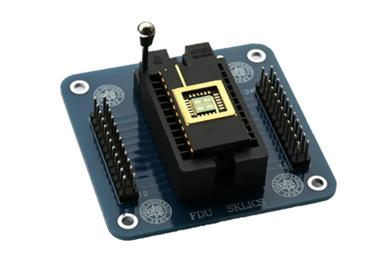
(Yicai) Oct. 9 -- Researchers from China's Fudan University have developed the world's first full-featured two-dimensional NOR flash memory chip, addressing key mass production challenges for new 2D information devices.
The new chip was created using an atomic device to chip technology, combining a superior 2D electronic device as a memory core and a powerful complementary metal-oxide-semiconductor platform to support complex instruction control, according to findings published in scientific journal Nature yesterday.
Demand for data storage in the artificial intelligence era is extremely high, requiring large capacity and very fast access speeds, which existing semiconductor charge storage devices are unable to meet, Liu Chunsen, a researcher from Fudan University's State Key Laboratory of Integrated Chips and Systems and corresponding author of the paper, told Yicai.
"The latest progress aims to solve key engineering challenges related to new 2D information devices and to push 2D flash memory products toward industrialization," Liu noted.
"It took around 24 years from the first prototype transistor to the birth of the first central processing unit," Liu pointed out. "By integrating advanced chip technology into the existing CMOS process platform, we have significantly compressed this process."
Building on previous research and integration efforts, the team taped out the chip. Next, they plan to establish an experimental base and collaborate with relevant institutions to set up a mass production process project using independently developed technology.
The team aims for the chip to achieve industrial-scale production within the next three to five years, initially targeting a capacity at the megabit level, Liu said, adding that once this is reached, they can utilize the large production lines of the project's industrial partners to manufacture the first batch of commercial products.
"Memory is the most likely type of 2D electronic device to be commercialized first because it does not have high material quality and manufacturing process requirements, while its performance indicators far exceed existing products," Zhou Peng, co-author of the paper and professor at Fudan University involved in the memory area for many years, said to Yicai. "Its widespread use could bring some disruptive new application scenarios."
Research on 2D semiconductors is still in its early stages and has not yet achieved mass applications. Since 2018, the team from Fudan University has made multiple groundbreaking advancements in the access speed of 2D flash memory devices, unveiling the PoX prototype device in April.
The PoX achieved an ultra-fast non-volatile storage speed of 400 picoseconds, making it the fastest semiconductor charge storage technology ever.
Editors: Tang Shihua, Martin Kadiev